Reverse Bias Circuit Diagram
A circuit that contains pure resistance r ohms connected in series with a pure capacitor of capacitance c farads is known as rc series circuit. As far as possible, the loop will not wrap around. Web in a standard diode, forward biasing occurs when the voltage across a diode permits the natural flow of current, whereas reverse biasing denotes a voltage across the diode in the opposite direction.
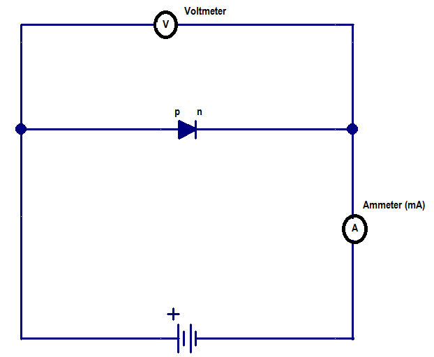
pn junction under reverse bias condition
Reverse Bias Circuit Diagram. Draw the output wavefrom across diode in given circuit. Generally, the interface device can be layout first, then the interface protection. Web in forward biasing the current is easily flowing through the circuit whereas reverse bias does not allow the current to flow through it.
A Simple Explanation Of Forward And Reverse Bias Of A Pn Junction.
The rc series circuit is shown in the figure below: Jaeger and blalock, microelectronic circuit design, mcgraw hill. Under reverse bias, the n side is held at a higher voltage than the p side.
A Sinusoidal Voltage Is Applied And Current I Flows Through The Resistance (R) And The Capacitance (C) Of The Circuit.
Web the reverse current in reverse bias condition is due to the minority carriers in the p and n regions. Web 556 views 3 years ago. Web 08 nov, 2021 follow diode is a simple electronic component that allows the flow of electric current in one direction while blocking it with high resistance in the other.
Diode In Reverse Biased Mode As Shown In Fig.
A circuit that contains pure resistance r ohms connected in series with a pure capacitor of capacitance c farads is known as rc series circuit. Generally, the interface device can be layout first, then the interface protection. Web how to reverse engineer a schematic from a circuit board:
Draw The Output Wavefrom Across Diode In Given Circuit.
Reverse bias increases a diode's resistance, and forward bias decreases a diode's resistance. As far as possible, the loop will not wrap around. The depletion layer of a diode is much thicker while in reverse bias and substantially thinner while in forward bias.
Web Since Each Junction Has Two Possible States Of Operation (Forward Or Reverse Bias) The Bjt With Its Two Junctions Has Four Possible States Of Operation.
The steps presented here are not exact, and you. If the applied voltage is v, then the total potential difference across the diode becomes v reverse bias = v 0 + v (where v 0 is the barrier potential). If the voltage moves in the opposite direction, we call that orientation a “reverse bias.” in reverse bias, current flow is nominally blocked as a sort of electronic check valve.
Web The Diagram Of Reverse Bias P N Junction Is Shown Below.
This results in the depletion region to be widened and the. In this case, the applied reverse potential acts in such a way that it establishes an electric field which increases the field due to the potential barrier. Web a reverse bias has a marginal forward current, while a forward bias has a significant forward current.
Understanding How These Diagrams Work And How They Can Be Used To Optimize Electrical Circuits Is Essential For Anyone Looking To Properly Design And Build Their Own Electronics.
Draw the truth table for the given logic gate. While reverse biasing helps too improve the time response of the photodiode to fast signals, it also reduces its sensitivity to very weak light signals, since the reverse bias voltage also drives a small leakage current across the pn junction. Web the main idea of circuit board schematic diagram reverse engineering should be according to the signal flow direction, so that the flow of the signal is as smooth as possible.
Use This As A Reference For Wiring The Components.
This article explains the construction, working, biasing, and everything else you need to know about the most fundamental analog electronic component. Web in forward biasing the current is easily flowing through the circuit whereas reverse bias does not allow the current to flow through it. However, the voltage present across a diode during reverse biasing does not produce any significant flow of current.
This Project Is A Result Of Needing To Service A Domestic Electronic Item Without Being Able To Obtain A Circuit Diagram.
Web the diagram above depicts the connections for the powerboost 1000c, audio amp, pitft, rotary switch, led and pi. In forward biasing the magnitude of the current depends on the forward voltage whereas in reverse bias the magnitude of the current is very small or negligible. The potential barrier is thus strengthened.
The Process Proved To Be Very Long And Painstaking, But Also Very Rewarding.
The 3.5 pitft connects to the raspberry pi. For a detailed description of the bjt structure see: Web in a standard diode, forward biasing occurs when the voltage across a diode permits the natural flow of current, whereas reverse biasing denotes a voltage across the diode in the opposite direction.
The Negative Side Of The External Bias Voltage Pushes The Minority Carriers In The P Region, Which Are Free Electrons, Toward The Pn Junction.

Solved 2 1. PN JUNCTION DIODE CHARACTERISTICS AIMTo

The Zener Diode Instrumentation and Control Engineering

PN Junction Diode and its Forward bias & Reverse bias characteristics

What is Reverse Bias p n Junction? Circuit Globe

Pn Junction Diode Quora

Forward Bias and Reverse Bias SPM Physics Form 4/Form 5 Revision Notes
Forward Biasing of a PN Junction Diode Manipal Made Easier

pn junction under reverse bias condition
